FABRICATION FACILITIES
Ion Milling
A Focused Ion Beam (FIB) – Scanning Electron Microscope (SEM) Dual Beam System allows the manufacture of complex patterns on the nanometre scale along with selective sputtering.
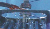
Multi-Source Sputtering (Separate system to above.)
Up to 4 materials can be sputtered at once allowing the deposition of multi-layers or compounds.
Deposition of thin-films by evaporation or spin-coating
Metal (e.g. gold, silver) and dielectric (e.g. silicon monoxide, PMMA, photoresist) can be deposited with film thickness being controlled with a precision of a few nanometres.
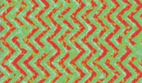
Manufacture of diffraction gratings
Both mono- and bi- diffraction gratings with groove pitches typically in the range 170nm to 2µm can be produced (longer pitch gratings can also be made).
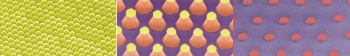
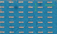
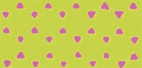
Manufacture of photonic surfaces
Arrays of spheroidal, triangular, rectangular or cylindrical particles and hole-arrays can be fabricated in metals or fused silica. The techniques used include: holography, nano-sphere lithography, electron beam lithography and etching.
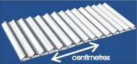
Manufacture of microwave surfaces
Extensive engineering facilities are available including a laser sinter system, CNC lathes and milling machines allowing the manufacture of surfaces and structures that diffract microwave radiation.
Rapid Thermal Annealing
A halogen lamp-based system allows samples to be heated to 500°C in less than 1 minute. A 60W laser annealing system is also available.
Liquid crystal cell fabrication
Facilities include a vacuum-filling system and rubbing machine (the latter being for preparation of liquid crystal-aligning layers.)
Langmuir-Blodgett (LB) film deposition
“Molecular staircases” with a step resolution of 5nm can be constructed. |